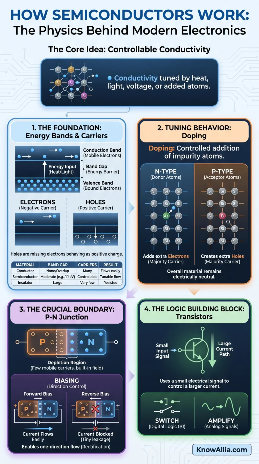
A semiconductor is a solid material whose electrical conductivity can be controlled. It does not behave like a metal, where many electrons move freely, and it does not behave like glass, where electrons are mostly locked in place. Its value comes from the middle ground: heat, light, voltage, and carefully added atoms can change how many charge carriers are available. That controllable behavior is why silicon and other semiconductor materials sit inside diodes, transistors, sensors, solar cells, memory chips, processors, and power electronics.[Source-a]
First, the Cleanest Mental Picture
Modern electronics work because engineers can guide tiny electric currents through patterned regions of semiconductor material. The physics is not magic. It is a chain of ideas: energy bands decide whether electrons can move, doping adjusts the number of available carriers, junctions steer current, and transistors use an electric signal to control a larger current.
- Band gap: the energy step an electron must cross to become mobile.
- Doping: the controlled addition of impurity atoms that create electrons or holes.
- Device action: the way junctions and electric fields turn controlled conductivity into useful switching, amplification, detection, or light conversion.
What a Semiconductor Is
A semiconductor is best understood as a controllable conductor. Pure silicon at room temperature conducts only a little, because most of its electrons are tied into covalent bonds. Add a small amount of the right impurity, shine light on it, heat it, or place it under an electric field, and the number of mobile charge carriers changes.
This is the main difference between a raw material and a useful electronic part. A piece of silicon is not automatically a processor. A chip is made by patterning many small regions so that some areas behave as n-type, some behave as p-type, some insulate, and some connect. The useful behavior comes from where each region is placed, not from silicon alone.
A simple analogy helps. A metal wire is like a road with open traffic all the time. An insulator is like a road with locked gates. A semiconductor is more like a road network with smart gates: the gates can be opened, narrowed, or closed by voltage, light, temperature, or material design.
- Conductors have many mobile electrons available with little added energy.
- Insulators have electrons that need much more energy before they can move freely.
- Semiconductors sit between those cases, so their conductivity can be shaped with precision.
How Energy Bands Control Conductivity
In a single atom, electrons occupy allowed energy levels. In a crystal, many atoms sit in an ordered lattice, and those levels spread into energy bands. The lower filled band is the valence band. The higher band where electrons can move through the crystal is the conduction band.
The empty energy range between them is the band gap. If an electron gains enough energy to cross this gap, it can join the conduction band and carry current. In silicon, the gap is often described as close to 1.1 eV at ordinary conditions; exact values vary with temperature and measurement context.[Source-b]
Useful detail: the band gap is not a physical crack inside the material. It is an energy interval where electrons cannot normally occupy stable states in the crystal. That is why light, heat, and voltage can change semiconductor behavior without breaking the material apart.
Electrons and Holes
When an electron leaves the valence band and becomes mobile, it leaves behind an empty state called a hole. A hole is not a tiny positive bead moving through the material. It is a missing electron in the bonding structure, yet it behaves mathematically like a mobile positive charge. That idea lets engineers describe current in p-type regions without tracking every individual electron step.[Source-c]
Both carriers matter. Electrons carry negative charge through the conduction band. Holes represent positive carrier motion in the valence band. Many devices work by controlling how these two carrier types are created, removed, separated, or recombined.
| Material Type | Band Behavior | Typical Carrier Availability | Electrical Result |
|---|---|---|---|
| Conductor | Allowed states make carrier motion easy. | Many mobile electrons are available. | Current flows readily. |
| Semiconductor | A moderate band gap must be crossed or modified. | Carrier count is controllable by doping, light, heat, and fields. | Current can be guided, switched, or sensed. |
| Insulator | The energy gap is too large for ordinary carrier motion. | Very few mobile carriers are available at normal conditions. | Current is strongly resisted. |
Why Doping Changes Everything
Doping means adding a very small amount of another element to a semiconductor crystal. The goal is not to make the material dirty. The goal is to place controlled electronic states near the bands so carriers can be created with far less energy than pure silicon would require.
In silicon, an atom such as arsenic has five valence electrons while silicon has four. Four electrons join bonds with neighboring silicon atoms, and the extra electron is weakly bound. OpenStax describes this impurity electron level as much closer to the conduction band than the full silicon energy gap, making it easy for room-temperature energy to free that electron.[Source-b]
N-Type and P-Type Silicon
Doping creates two main material behaviors:
- N-type semiconductor: donor atoms provide extra electrons. Electrons are the majority carriers.
- P-type semiconductor: acceptor atoms create holes. Holes are the majority carriers.
- Minority carriers: the less common carrier type still exists and matters in diodes, transistors, sensors, and solar cells.
The material remains electrically neutral overall. N-type does not mean the whole crystal has a net negative charge, and p-type does not mean it is simply positively charged. It means one carrier type is easier to use for current.
| Region | How It Is Made | Majority Carrier | What It Enables |
|---|---|---|---|
| N-type | Donor atoms add loosely bound electrons. | Electrons | Electron-rich regions for junctions, channels, and contacts. |
| P-type | Acceptor atoms create empty states in the bonding structure. | Holes | Hole-rich regions for junctions, transistor bodies, and device control. |
| Intrinsic semiconductor | Very pure material with no deliberate dopant pattern. | Electrons and holes mainly from thermal excitation. | A reference case; useful for understanding the physics before device design. |
Example: a silicon diode is not made by using only “better conducting silicon.” It needs a boundary between p-type and n-type regions. The boundary is where the useful one-direction behavior appears.
The P-N Junction: Where Direction Appears
A p-n junction forms when p-type and n-type semiconductor regions meet. Electrons from the n-side and holes from the p-side diffuse near the boundary and recombine. This leaves charged donor and acceptor ions fixed in the crystal. The result is a thin depletion region, a zone with very few mobile carriers.[Source-d]
That depletion region creates an internal electric field. The field acts like a built-in barrier. It does not block all motion forever, but it decides how easily current can pass depending on the applied voltage direction.
Forward and Reverse Bias
- Forward bias: the external voltage lowers the barrier. Carriers cross the junction more easily, so current can flow.
- Reverse bias: the external voltage widens the effective barrier. Only a small leakage current flows under normal conditions.
- Rectification: because current passes much more easily in one direction, a diode can convert alternating current behavior into one-direction current behavior in many circuits.[Source-e]
This one-direction behavior is one of the first useful tricks of semiconductor physics. Once a junction can steer current, more complex devices can switch, amplify, sense light, emit light, and store information.
How Semiconductor Control Builds Electronics
A device is useful when carrier motion is controlled in the right place, at the right time, and in the right direction.
Carrier Control Path
1. Energy Bands
The band gap sets how hard it is for electrons to become mobile.
2. Doping
Donor and acceptor atoms make electrons or holes easier to use.
3. Junctions
P-type and n-type regions create barriers that steer current.
4. Transistors
A small signal controls a larger current path, so circuits can switch and process information.
Device Outcomes
Uses one p-n junction to favor current in one direction.
Uses light-generated carriers and a junction field to separate charge.
Uses gate voltage to form or remove a conductive channel.
Combines many patterned devices and metal connections on one chip.
Energy Selectivity
Only electrons with enough energy can cross into mobile states.
Spatial Patterning
The same wafer contains many regions with different electrical roles.
Signal Control
Small voltages can guide much larger circuit behavior.
How Transistors Turn Physics Into Logic
A transistor is a semiconductor device that uses one electrical signal to control another. This is why it can act as a switch in digital circuits and as an amplifier in analog circuits. The device does not create energy. It controls energy supplied by the circuit.
There are several transistor families, but two ideas are enough for a clear start: a bipolar junction transistor uses carrier injection across junctions, while a MOSFET uses an electric field from a gate electrode to control a channel. In both cases, small control changes create large circuit effects.
Bipolar Junction Transistor
A junction transistor has three regions. In an n-p-n transistor, the regions are emitter, base, and collector. A small base current can control a larger current between the emitter and collector, which is why older textbooks often describe it as a controllable valve for current.[Source-d]
The important point is not the label on each terminal. The important point is carrier control. The device is shaped so that a small input condition changes how easily carriers move through the main path.
MOSFET
The MOSFET is the workhorse of modern digital chips. Its gate is separated from the semiconductor by a very thin insulating layer. When gate voltage is applied, the electric field changes the carrier population under the gate. A conductive channel can form, allowing current between source and drain. Remove or change the voltage, and the channel can shrink or disappear.
This is why digital logic can represent 0 and 1 with electrical states. A transistor does not need a moving mechanical part. It switches by reshaping electric fields and carrier density inside a tiny region of material.
How Chips Use the Same Physics Many Times
A microchip is not one semiconductor device. It is a carefully patterned system of many devices, insulating layers, and metal connections. Semiconductor manufacturing repeats steps such as layer growth, lithography, etching, deposition, doping, and metallization across a wafer. NIST describes photolithography as a process used to fabricate integrated circuits and as a long-running enabler of microelectronics progress.[Source-f]
The word lithography can sound abstract, but the basic idea is direct: use light and patterned masks to define where material should remain, where it should be removed, and where later steps should change the wafer. After many patterned layers, the chip contains transistors, contacts, and wiring stacked into a working circuit.
Material, Device, and Chip Are Not the Same Thing
- Material: silicon, gallium arsenide, silicon carbide, gallium nitride, or another semiconductor with suitable band behavior.
- Device: a diode, transistor, sensor, LED, or solar cell made by shaping carrier motion.
- Chip: many devices and connections arranged on one die to perform a circuit function.
This distinction matters because “semiconductor” can mean the material itself, a device made from it, or an industry term for chips. In physics, the material behavior comes first. In electronics, the engineered pattern is what turns that behavior into work.
Light, Heat, and Power Electronics
The same band-gap idea explains several familiar technologies. In a solar cell, light can create electron-hole pairs when photon energy is suitable for the semiconductor. The Department of Energy notes that a photovoltaic semiconductor’s band gap affects which wavelengths of light the cell can absorb and convert into electrical energy.[Source-g]
In an LED, electrons and holes recombine and release energy as light. The semiconductor material and its band gap help determine the emitted color. In power electronics, materials such as silicon carbide and gallium nitride are valued because their wider band gaps can support high voltage, high temperature, or faster switching in suitable designs.
Temperature also matters. Heating a semiconductor can create more electron-hole pairs, which changes conductivity. That is useful in some sensors but must be managed in processors and power devices, where excess heat can affect speed, leakage, reliability, and energy use.
Terms Worth Knowing
- Band Gap
- The energy difference between the valence band and conduction band.
- Valence Band
- The band where electrons are usually tied to bonds in the crystal.
- Conduction Band
- The band where electrons can move through the crystal and carry current.
- Dopant
- An added atom that changes carrier availability in a controlled way.
- Donor
- A dopant that can provide an extra electron, creating n-type behavior.
- Acceptor
- A dopant that creates a hole, leading to p-type behavior.
- Depletion Region
- A carrier-poor region near a p-n junction with a built-in electric field.
- Channel
- The controlled path where current flows in many field-effect transistors.
- Leakage Current
- A small unwanted current that can flow even when a device is meant to be off.
Common Misconceptions and Confusion
“Silicon Is Automatically a Good Conductor”
Pure silicon is not used like copper wire. Its value is that conductivity can be tuned. The useful behavior appears after purification, doping, patterning, contacts, and device design.
“Holes Are Little Positive Electrons”
A hole is an empty electronic state that behaves like a positive carrier. It is a valid and useful model, but it should not be confused with a separate positive particle moving through empty space.
“Doping Means Random Contamination”
Doping is controlled. The type, amount, location, and activation of dopants are chosen so the device has the needed carrier behavior. Random contamination is a problem; engineered doping is a design tool.
“Transistors Create Current From Nothing”
A transistor controls a current supplied by the circuit. It can switch or amplify, but the energy comes from the power source. The semiconductor structure lets a small signal control a larger flow.
What the Simple Model Leaves Out
The explanation above is accurate for the main ideas, but real semiconductor engineering adds more detail. Actual devices depend on crystal defects, surface states, oxide quality, contact resistance, carrier mobility, quantum effects, thermal design, manufacturing variation, and packaging. At nanometer scale, the behavior can no longer be described only by simple pictures of electrons crossing a junction.
Another limit is that no single material is best for every job. Silicon is widely used because it is well understood and manufacturable, but other semiconductors are chosen when light emission, high-frequency behavior, high voltage, or heat tolerance matters more than general-purpose chip density.
A Short Historical Note
The transistor became a defining device of electronics after mid-20th-century semiconductor research. The Nobel Prize in Physics 1956 was awarded to William B. Shockley, John Bardeen, and Walter H. Brattain for research on semiconductors and discovery of the transistor effect.[Source-h] The Computer History Museum describes the first point-contact transistor demonstration in 1947 and the later junction transistor work that followed.[Source-i]
That history matters because it shows the central pattern of semiconductor progress: better control of materials creates better control of current. The devices have changed shape many times, but the physics still starts with bands, carriers, fields, and junctions.
Questions People Ask About Semiconductors
Semiconductor FAQ
Why Are Semiconductors Used Instead of Ordinary Conductors?
Conductors are useful for carrying current, but they do not naturally give precise control over current flow. Semiconductors can be patterned and doped so that voltage, light, heat, and electric fields change their behavior. That controllability makes switching and sensing possible.
What Is the Most Common Semiconductor Material?
Silicon is the most common semiconductor material in computer chips and many solar cells. It is abundant, forms a useful oxide, and has a long manufacturing history. Other materials are used when a device needs special optical, power, or high-frequency behavior.
What Does the Band Gap Do?
The band gap sets the energy needed for electrons to become mobile. It affects conductivity, light absorption, light emission, leakage current, and temperature behavior. A smaller or larger band gap can be useful depending on the device.
Is Doping the Same as Damaging the Semiconductor?
No. Doping is a controlled material process. It adds selected atoms in selected regions to create n-type or p-type behavior. Damage and unwanted contamination are different problems that engineers try to avoid.
Why Do Diodes Conduct in One Direction?
A diode contains a p-n junction with a depletion region. Forward bias lowers the barrier and allows much more current to pass. Reverse bias raises the effective barrier, so only a small leakage current flows under normal conditions.
Why Are Transistors So Important in Computers?
Transistors can switch between electrical states without moving mechanical parts. When many transistors are patterned and connected on a chip, they can form logic gates, memory cells, processors, and control circuits.
Sources
- [Source-a] NIST – Semiconductors — Used for the definition of semiconductors as tunable-conductivity materials used in integrated circuits.
- [Source-b] OpenStax – University Physics Volume 3, 9.6 Semiconductors and Doping — Used for band gap, donor impurities, acceptor impurities, and n-type/p-type explanations.
- [Source-c] Encyclopaedia Britannica – Hole, Solid-State Physics — Used for the explanation of holes as positive carrier behavior created by missing electrons.
- [Source-d] OpenStax – University Physics Volume 3, 9.7 Semiconductor Devices — Used for p-n junction behavior, depletion layer formation, and transistor basics.
- [Source-e] Encyclopaedia Britannica – P-N Junction — Used for rectification and current direction in p-n junctions.
- [Source-f] NIST – Polymers for Next-Generation Lithography — Used for photolithography as a process used to fabricate integrated circuits.
- [Source-g] U.S. Department of Energy – Solar Photovoltaic Cell Basics — Used for the role of band gap in photovoltaic light absorption and conversion.
- [Source-h] Nobel Prize – The Nobel Prize in Physics 1956 — Used for the Nobel-recognized transistor-effect discovery.
- [Source-i] Computer History Museum – Inventing the Transistor — Used for the first transistor demonstration and early transistor development context.